As an Amazon Associate, we earn from qualifying purchases. Some links on this site are affiliate links at no extra cost to you. Our recommendations are based on thorough research and editorial judgment.


How Are Solar Panels Made? Inside the Manufacturing Process

I start with quartz and carbon at ~1,400 °C to produce metallurgical‑grade silicon (~98 % purity), then react it with chlorine at 300 °C forming trichlorosilane, which is distilled and reduced with hydrogen at 1,200 °C to achieve electronic‑grade silicon containing fewer than 10 ppb impurities, while recycling chlorine cuts waste and cost; the purified melt is transferred into a quartz crucible heated to 1,420 °C, where a seed crystal is introduced, crucible rotates 2–3 rpm, seed spins at 5 rpm, and the ingot is pulled at 1 mm min⁻¹ with a 10 °C cm⁻¹ gradient, yielding a 180 mm × 2 m crystal with dislocation density below 10³ cm⁻² and oxygen 200‑400 ppm, after which diamond‑wire slicing at 0.5 mm s⁻¹ and 15 kHz oscillation creates 180 µm wafers with ±2 µm uniformity, followed by colloidal‑silica polishing at 30 rpm producing Ra < 0.05 µm surfaces, phosphorus diffusion at 900 °C for 30 s implants 1×10¹⁸ cm⁻³ donors, KOH texturing yields <5 % reflectance, screen‑printed silver and aluminum contacts are fired at 750 °C, and finally cells are laminated at 150 °C under 0.5 MPa, inspected, and certified, leading to the next detailed steps.
Key Takeaways
- High‑purity silicon is produced by converting quartz with carbon, then refining via trichlorosilane chemistry and hydrogen reduction to reach <10 ppb impurities.
- Single‑crystal ingots are grown by the Czochralski method, pulling a seed from molten silicon at ~1,420 °C with controlled rotation and temperature gradient.
- Ingots are sliced into wafers using a diamond‑wire saw, then polished to sub‑0.05 µm surface roughness and cleaned ultrasonically.
- Doping (phosphorus diffusion) creates n‑type regions, surface texturing reduces reflectance, and silicon nitride passivation is applied before metallization with silver and aluminum contacts.
- Cells are interconnected, laminated with EVA and a backsheet, then thermally cured and tested for durability and performance before certification.
How Quartz Turns Into High‑Purity Silicon for Solar Panels
When quartz is heated to approximately 1,400 °C in a furnace, it reacts with carbon to produce metallurgical‑grade silicon, a material that contains roughly 98 % purity and serves as the initial feedstock for solar‑cell manufacturing. I then introduce chlorine gas, which reacts with the silicon at 300 °C to form trichlorosilane, a volatile intermediate that enables precise impurity removal; this step, coupled with chlorine recycling, reduces waste and lowers operational cost. The trichlorosilane is distilled, purified, and reduced with hydrogen at 1,200 °C, yielding electronic‑grade silicon with impurity concentrations below 10 ppb, a specification critical for achieving solar‑cell efficiencies above 20 %. Throughout, feedstock sourcing is monitored, ensuring quartz quality meets ASTM C 1155 standards, while process controls maintain temperature stability within ±5 °C, guaranteeing consistent product quality.
Growing Single‑Crystal Ingots for Solar‑Panel Cells With the Czochralski Method
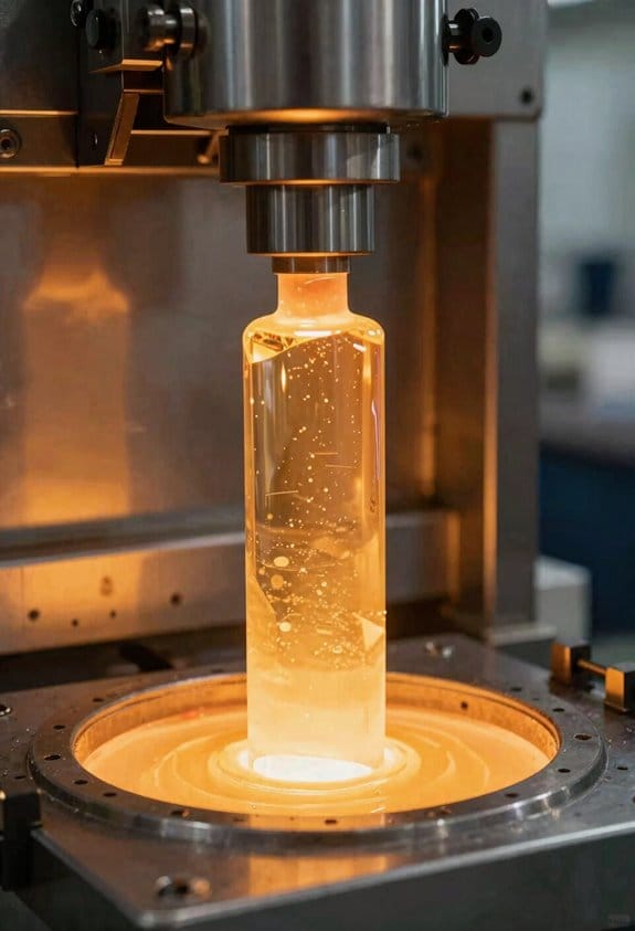
After purifying quartz into electronic‑grade silicon for modules used in home solar power systems, I load the molten silicon into a quartz crucible, heat it to 1,420 °C, and introduce a seed crystal while rotating the crucible at 2–3 rpm. The seed rotation, typically set at 5 rpm, guarantees uniform axial growth, while the crucible atmosphere is continuously filtered to prevent crucible contamination that could introduce metallic inclusions. As the crystal pulls upward at 1 mm min⁻¹, the temperature gradient is maintained at 10 °C cm⁻¹, producing a cylindrical ingot of 180 mm diameter and 2 m length, which yields a dislocation density below 10³ cm⁻², essential for high‑efficiency cells. I monitor oxygen incorporation, adjusting the ambient argon flow to keep oxygen content between 200–400 ppm, thereby balancing mechanical strength and electrical performance without compromising crystal uniformity.
Cutting and Polishing Wafers to Mirror Finish for Solar‑Panel Production
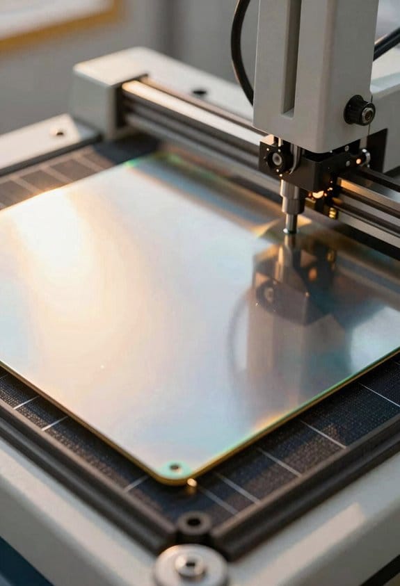
I begin by positioning the ingot on the multi‑axis slicing platform, aligning it so that the diamond‑wire saw—operating at 0.5 mm s⁻¹ feed rate, 15 kHz oscillation frequency, and 2 % coolant flow—cuts the crystal into wafers of 180 µm thickness, maintaining ±2 µm uniformity across the 156 mm × 156 mm sheet, while simultaneously monitoring kerf loss, which typically remains below 0.05 mm, and ensuring that the resulting wafer edges exhibit a surface roughness (Ra) under 0.5 µm, a prerequisite for subsequent polishing steps that will achieve a mirror finish with reflectivity exceeding 99 % in the visible spectrum. After slicing, I load wafers into a rotary polishing system, where slurry containing colloidal silica removes micro‑scratches, while periodic ultrasonic cleaning eliminates chemical residues; the process, controlled at 30 rpm, 45 µm particle size, and 0.8 % pH, yields a surface Ra below 0.05 µm, preventing edge chipping, and the final inspection verifies reflectivity and dimensional tolerances before downstream cell fabrication.
Doping, Texturing, and Adding Contacts to Form Solar Cells
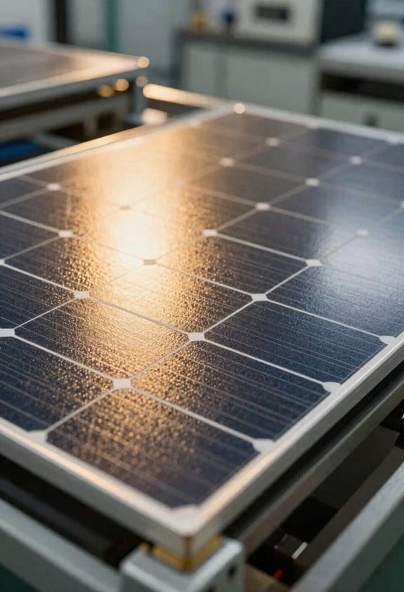
I’ll begin by introducing phosphorus into wafers destined for portable solar panels or rooftop modules, which involves exposing the wafer to a phosphine (PH₃) atmosphere at 900 °C for 30 seconds, allowing phosphorus atoms to diffuse into the n‑type layer to achieve a donor concentration of roughly 1 × 10¹⁸ cm⁻³, while simultaneously monitoring sheet resistance to stay within 5 Ω sq⁻¹ tolerance. After doping, I etch a random pyramidal texture using a mixture of potassium hydroxide and isopropyl alcohol, creating micrometer‑scale facets that reduce reflectance below 5 % across the solar spectrum, thereby enhancing photon capture and extending carrier lifetime by minimizing surface recombination. Subsequently, I deposit a thin silicon nitride layer for surface passivation, which simultaneously serves as an antireflection coating, then screen‑print silver front contacts and aluminum rear paste, fire the assembly at 750 °C for 10 minutes to alloy the metals, and verify contact resistivity below 0.1 Ω·cm² before proceeding to cell testing.
Joining Cells Into Strings and Laminating Panels Into Complete Solar Modules
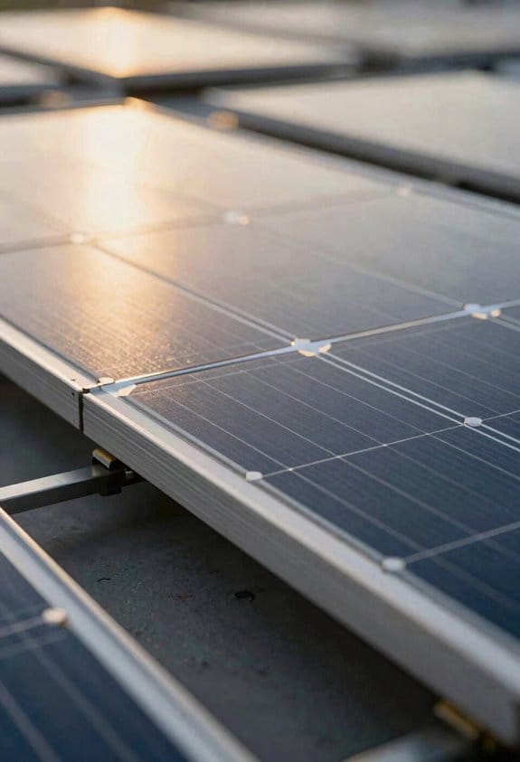
Cell strings are assembled by laser‑cutting individual wafers into half‑cell or third‑cell pieces, then soldering thin copper ribbons—typically 0.2 mm wide and 30 µm thick—along the front and rear contacts, which yields a series connection that raises module voltage to 30–40 V while keeping current below 10 A, and the resulting strings are laid on an ethylene‑vinyl acetate (EVA) sheet, spaced 2–5 mm apart to accommodate thermal expansion, before a second EVA layer and a polymer backsheet are added, a step that guarantees mechanical stability, moisture protection, and electrical insulation. I then align the glass, EVA, cell strings, and backsheet in a laminating press, heat the assembly to 150 °C for 15 minutes to initiate EVA curing, and apply 0.5 MPa pressure, ensuring uniform adhesion, while monitoring ribbon soldering integrity, and after cooling to room temperature the panel retains a flat, void‑free structure ready for framing and electrical interconnection.
Recommended Products

Protect important documents, surfaces, text books and more

Laminating Pouches Dimensions: 660 PACK 9" x 11.5"laminating sheets ,3 mil thickness , fits for 8.5 x 11 inch document and photos

Matte Finish Design: the matte self adhesive laminating sheets adopt a matte finish design that effectively reduces glare, prevents dirt, fingerprints, and scratches, making them very suitable for frequent use; They can perfectly display your photos and laminated works
Final Testing, Durability Checks, and Certification of Solar Modules
Because the panel has been laminated and framed, the next step is to verify that it meets performance, reliability, and safety standards, which involves a series of electrical, environmental, and mechanical tests performed under controlled conditions. I run a 1000‑hour thermal cycling test from –40 °C to +85 °C, monitoring power loss, then conduct a 500‑hour humidity‑freeze test at 85 % relative humidity, checking for delamination and corrosion, while simultaneously measuring open‑circuit voltage, short‑circuit current, and maximum power point to ensure they stay within ±5 % of rated values. After passing these, I perform field testing on a 1 MW farm to validate real‑world output, then submit data for certification, confirming warranty validation criteria such as a 25‑year performance guarantee and IEC 61215 compliance.
Recommended Products

Withstands drops up to 4-meters (13 feet) with industrial strength casing and holster

Portability and Versatility: Newpowa 200W Portable Solar Panel with an expanded size can be folded into an ultra-compact size. Coming standard with a durable carry- handle, this panel can be easily folded and carried anywhere you go. This panel is great for RVs, camping, hiking, and much more.

TÜV Certification Qualification: TÜV certified under IEC 61215, IEC 61730 and UL 61730. Independently tested for durability, electrical and mechanical safety, perfect for RV, marine, rooftop and off-grid installations.
Frequently Asked Questions
What Is the Environmental Impact of Silicon Purification?
I’m aware that silicon purification devours massive energy, and the chlorine‑based chemicals can cause water pollution if not properly treated, so I always stress stricter waste‑management and renewable‑energy sourcing to cut those impacts.
How Are Waste Gases From Trichlorosilane Production Managed?
I capture the trichlorosilane off‑gases with scrubber systems, then feed the cleaned streams into gas recycling loops—don’t you think that turns waste into a resource while cutting emissions?
Why Do Some Panels Use Polycrystalline Instead of Monocrystalline Cells?
I choose polycrystalline cells because they’re lower cost and generate less waste during crystal growth, so you get decent efficiency without the pricey, high‑purity silicon needed for monocrystalline panels.
What Are the Typical Failure Modes Detected by Double‑El Testing?
I tell you double‑EL testing spots microcrack mapping and series resistance spikes, revealing hidden cell fractures and interconnect failures that can quickly degrade panel performance.
How Does Panel Framing Affect Long‑Term Durability?
I find that sturdy framing boosts durability by ensuring even load distribution and reliable edge sealing, which prevents moisture intrusion and stress concentration, so the panel maintains performance and resists cracking over years.